Hi friends,
This newsletter we’re streamlining the process of creating circuit boards and revisiting the DIY electronic calipers project from two years ago.
Kevin’s KiCad Helpers
I first started playing around with electronics via Arduino back in 2010, and I designed my first circuit board back in 2015 for my walnut and leather cell phone. Since then, I’ve made around a dozen PCBs, with a notable spike during the pandemic making weird mechanical keyboards.
Averaging roughly one PCB/year is a maximally frustrating frequency: I have 100’s of hours of cumulative experience, but it’s sufficiently spread across the forgetting curve that every time I start something the details are only vaguely familiar and I’ve got to re-orient myself again. It reminds me of filling out my taxes, where I also furiously consult my notes and attempt to interpret them against new versions of the UI where input boxes have been hidden across other forms and new sub-menus.
Anyway, armed with a coding agent, I externalized everything I kept forgetting how to do in a pile of scripts: Kevin’s KiCad Helpers.
This is tailored to my needs — designing PCBs in KiCad 10 to be manufactured by JLCPCB — but if yours are similar you might find ‘em helpful. Even if you don’t make PCBs, it might be good inspiration for how to apply LLMs to sand down rough edges of whatever convoluted infrastructure is required for your projects.
A quick tour of the tools:
DXF import
I specify all of my mechanical stuff — board outlines, mounting hole positions, etc. — in Autodesk Inventor since it has a constraint solver and allows me to directly reference complex geometry driven by other objects.
KiCad’s GUI has a DXF import tool, but it doesn’t have a mechanism to replace already imported geometry, which makes it tedious to iterate.
This script:
- imports geometry from a DXF file into a board layer specified by the filename (
panel_Edge.Cuts.dxfimports a group ID’d “panel” to the Edge Cuts layer) - deletes any geometry previously imported with that ID
- polls the file for changes, so you get “live reload”
I combine this with a similar poll + export-to-file script in my mechanical CAD tool (shown above) to get live syncing to KiCad (shown below):
DXFs map into KiCad’s origin at top-left of the page outline and the DXF positive Y direction points up, so most of my PCBs end up drawn outside of the page ¯\_(ツ)_/¯.
STEP export
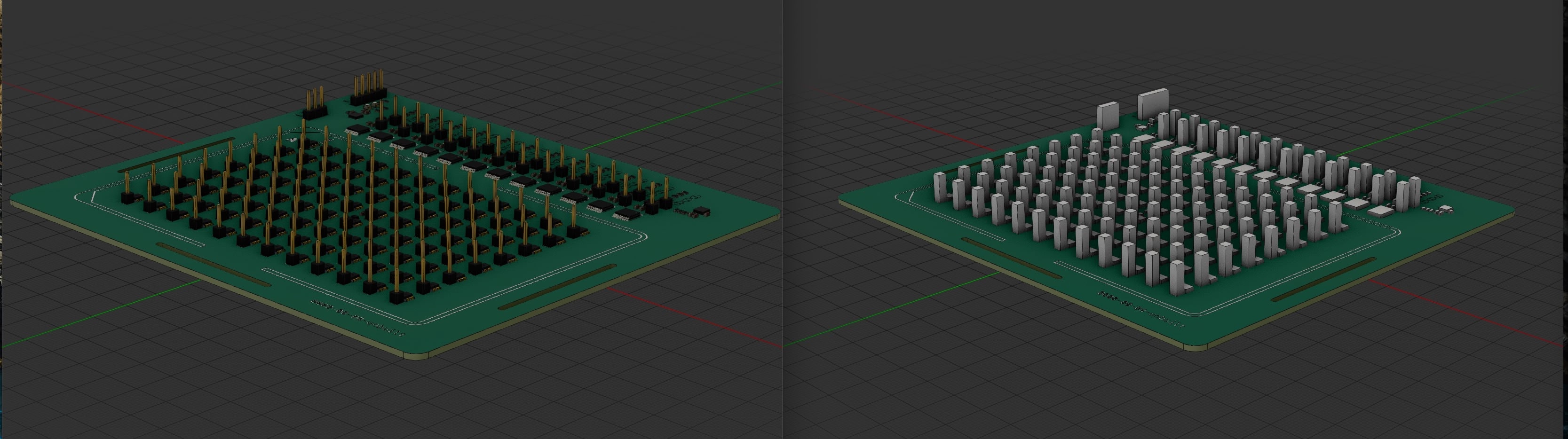
I also need the reverse direction: Import a 3D model of a circuit board and its components back into my mechanical CAD program so I can verify clearances, etc. KiCad has native STEP export, but unfortunately some of the parts have extremely detailed 3D models. My M1 Macbook Air running Windows CAD software in a virtual machine does not do well when every pin of every chip is a separate solid body.
This script generates a STEP export where all parts have been replaced with axis aligned bounding boxes:
Parts database
I design all of my boards to be assembled by JLCPCB, so it’s extremely helpful to have a low-latency way to query their parts. This script downloads CDFER’s daily JLCPCB parts sqlite database and consolidates everything into a single table with a numeric price column and lots of indexes so that searching is fast:
I use DB Browser for SQLite but you can of course use whatever interface you like.
It’s also extremely useful to point LLM agents at this database:
My dude, I need an H-bridge that can drive +/- 30 Volts, please query ~/foo/bar/parts.db and give me a table with 5 options for integrated ones showing price / stock / description. Please also make a table showing options for drivers with external transistors. Include links to the datasheets.
JLCPCB (EasyEDA) schematic and footprint import
Shout out again to CDFER for their JLCPCB KiCad Library, which has all of the “basic” jellybean parts and some of the extended ones as well.
For the parts that are not already available in here, I need to import them. Rather than draw them entirely from scratch, I use uPesy’s easyeda2kicad.py.
However I don’t always want to create an entirely new symbol and footprint if the part actually corresponds to something that’s in the KiCad standard library. So my import tool tries to match existing footprints (including 90 degree rotations) and spawns a terminal UI so you can interactively compare potential matches with the EasyEDA footprint:
Schematic analysis
The most interesting helper I’ve created so far is a general schematic analysis framework, which imports the KiCad netlist and schematic instance properties into a DataScript graph database to run various queries/checks.
For example, this lil’ function calculates the capacitance (of all the explicit capacitors, anyway) on a given net:
(defn net-capacitance
  [db net-name]
  (some->> (d/q '{:find  [?ref ?v]
                  :in    [$ ?net]
                  :where [[?n :net/name ?net]
                          [?n :net/nodes ?node]
                          [?node :node/pin ?pin]
                          [?i :instance/pins ?pin]
                          [?i :instance/ref ?ref]
                          [(clojure.string/starts-with? ?ref "C")]
                          [?i :instance/value ?v]]}
                db net-name)
           (keep (comp parse-capacitance second))
           seq
           (reduce + 0.0)))
This function can then be used to check the total capacitance on, e.g., the power nets, and throw an error if it exceeds, e.g., the maximum 10uF allowed by the USB specification.
(defn check-total-capacitance!
  [db]
  (let [rows (->> ["VCC" "VBUS"] ;;TODO: make this configurable
                  (keep (fn [net]
                          (when-let [c (net-capacitance db net)]
                            {:net net :total-uF (format "%.2f" (* c 1e6))}))))]

    (when (seq rows)
      (print "total capacitance:")
      (clojure.pprint/print-table rows)

      (doseq [{:keys [net total-uF]} rows]
        (assert (< (Double/parseDouble total-uF) 10) (str "Net " net " exceeds USB spec 10uF capacitance"))))))
(It’s easy to accidentally exceed this limit if you keep incrementally adding ICs and their recommended bypass capacitors.)
Since KiCad allows one to add arbitrary key/value pairs to schematic instances, it’s easy to check and print other data as well.
For example, I record the i2c address(es) of each chip this way (note i2c and max_mA fields in property inspector on left):
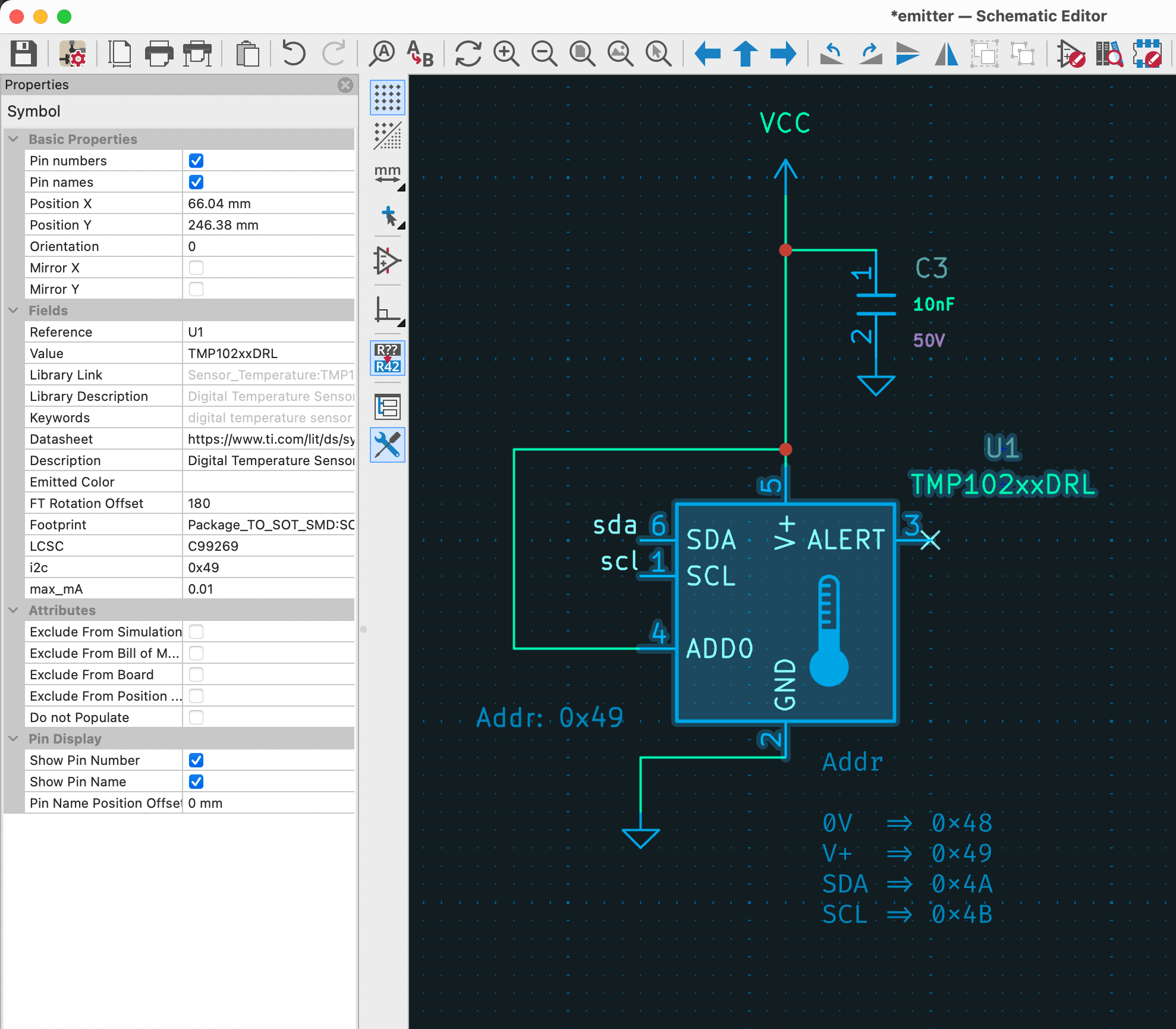
Within the schematic text labels I reference using the KiCad text variable format.
(E.g., the above Addr: 0x49 label is defined as Addr: ${U1:i2c}.)
The analysis script throws an error if an address maps to multiple chips:
(defn i2c-addresses
  [db]
  (d/q '{:find [?hex-addr (distinct ?ref)]
         :where [[?instance :instance/ref ?ref]
                 [?instance :instance/attributes ?attribute]
                 [?attribute :attribute/name "i2c"]
                 [?attribute :attribute/value ?addrs]
                 [(clojure.core/identity ?addrs) [?addr ...]]
                 [(clojure.core/format "0x%x" ?addr) ?hex-addr]]}
       db))


(defn check-i2c!
  [db]
  (let [refs-by-addr (i2c-addresses db)]
    (when (seq refs-by-addr)
      (print "i2c addresses")
      (clojure.pprint/print-table (sort-by :addr (for [[addr refs] refs-by-addr]
                                                   {:addr addr :refs (clojure.string/join " "  (sort refs))})))

      (doseq [[addr refs] refs-by-addr
              :when (< 1 (count refs))]
        (throw (ex-info (str "Addr " addr " matches multiple refs: " refs)
                        {:addr addr :refs refs})))

      (println ""))))
This also prints out a helpful table of everything on the bus every time I build the project:
| :addr | :refs |
|-------+-------|
|  0x20 |    U3 |
|  0x49 |    U1 |
|  0x60 |    U2 |
|  0x61 |    U2 |
|  0x62 |    U2 |
|  0x63 |    U2 |
|  0x64 |    U2 |
|  0x65 |    U2 |
|  0x66 |    U2 |
|  0x67 |    U2 |
|  0x68 |    U2 |
|  0x69 |    U2 |
|  0x6a |    U2 |
|  0x6b |    U2 |
|  0x6c |    U2 |
|  0x6d |    U2 |
|  0x6e |    U2 |
(In this example, U2 is an LED driver and exposes each channel on its own i2c address, so its i2c property is specified as 0x60..0x6F.)
Check/build scripts
Speaking of builds, most of the functionality described above is packaged up as a script, so you just run kkh build in a folder and it’ll create an output directory next to every *.kicad_pro it finds in any subfolder.
The outputs are named with the date, git revision, and also indicate whether there are unstaged changes in the repository working tree:
2026-07-07-73c5c1
├── bom.csv
├── designators.csv
├── netlist.ipc
├── positions.csv
├── receiver-gerbers-2026-07-07-73c5c1.zip
├── receiver.full.step
├── receiver.simplified.step
└── schematics
    ├── receiver-pcb-back.pdf
    ├── receiver-pcb-front.pdf
    └── receiver-sch.pdf
So one command runs DRC, ERC, and custom analysis checks and then builds all of the output files required to place a JLCPCB assembly order.
The build script also exposes the version string as a KiCad variable, so if you add ${KKH_VERSION_DATE} to your PCB silkscreen, the actual version will appear in the output Gerber files.
I hope by making a proper build script I will never again relive the shame of forgetting to run ERC and having a PCB manufactured where I literally forgot to connect some IC pins entirely…
Caliper updates
About two years ago I had my first foray into digital signal processing and made some electronic calipers.
I haven’t touched the project since I published that post, but a few folks recently asked me about it, and since I had some spare LLM credits I figured I’d spend five minutes sending off the little dude at the problem.
And I literally mean five minutes — these are very rough, rambly dictated prompts that I didn’t even bother to edit. I’m sharing here to remind everyone (especially myself!) that not everything needs to be A Big New Project and sometimes you can have great success from a quick, low-effort attempt.
I spawned a Claude session in the project repo, dictated the following prompt, and went to brush my teeth:
This is a project that I worked on a while ago and the accuracy that came out was alright but I’m wondering if there’s anything I can do to improve the accuracy purely from a computational way rather than making new hardware. Be sure to read the blog post mentioned at the top of the read me to get a background
After I brushed my teeth, it had come up with a few plausible sounding ideas, so I replied with the following and went to sleep:
I’d like you to set this up and come up with a few different ideas. These are pretty good ones and what I want you to do is Wire them up so that I can test them out Individually as a series of experiments with a given protocol and I want you to set everything up as much as possible So I can do it Quickly on my end without having to get in and change the code or anything like that so what you can do is you can make a branch and then Have maybe different entry points or something for each of these different improvements and then Write like an overall program or something like that Which I can just run to test through it and then make it interactive I guess so that I can You know start it up in the hardware Let it sit still for a certain amount of time Move it a fixed amount and back and then You know or some protocol like that and then I’ll tell you what I’m done and then we can just run through that program To test out all of the different ideas and potentially combinations of ideas in like a 10 or 15 minute setting and then We’ll figure out from that which ones are working most effectively
Again, I’m really not trying that hard here.
I woke up the next morning and spent about 20 minutes setting up the caliper PCBs and then running the programs it generated to collect new measurement data. It tried the following improvement hypotheses (LLM-generated text):
| knob | idea it tests |
|---|---|
| window size | longer coherent integration (noise ∝ 1/√N), incl. one 50 Hz line period |
| mean_sub | remove DC so ADC offset drift can’t leak into the phase |
| hann | suppress spectral leakage from non-integer-cycle windows |
| smoothing | averaging in I/Q (phasor) space instead of phase space; EMA vs block |
| hysteresis | the current 0.1 rad dead-band vs smaller vs none |
and based on the initial results and a bit more chatting, the agent proposed an improvement that is, of course, completely obvious in hindsight. My initial parameter sweep (two years ago) used a fixed 2kHz spacing. However, the actual signal and sampling timings generated by the microcontroller are driven by integer divisions of a fixed clock frequency — so most of these sampled timings don’t “line up” nicely in terms of an integer number of signal periods.
Thus, there’s always a bit of DC bias in the signal, which causes undesired noise.
With this change, the LLM-generated experimental code reports a noise floor of around 50um, which is about 10x better than what I was getting before. I’m currently on holiday away from my lab, but I expect it’ll take 30 minutes once I get back to code it up myself and validate.
Anyway, the main takeaways for me are:
- Write up your work in blog posts so that both people and LLMs can quickly get context and help you out
- There’s still plenty of low-hanging fruit out there to pick, and with LLMs it’s extremely cheap to just ask
Misc. stuff
Accidental anonymity “Sorry to say it but if you need your work to be polished and beyond reproach, that’s a determination and character problem, not a skill problem.”
High Performance Motor Control From the Ground Up || Field Oriented Control (FOC)
Bio-Rad Laboratories Helios® Gene Gun sounds like a joke, but it’s absolutely real and I desperately want to use it.
I didn’t build a Full Body Ultrasound… but I know the people that did
AgentsView is a very nice local web UI from my friend Wes McKinney that makes it easy to review transcripts and token usage across Claude Code, Codex, etc. I used it to quote some of my LLM sessions above.